1. Basic Properties and Nanoscale Habits of Silicon at the Submicron Frontier
1.1 Quantum Arrest and Electronic Structure Makeover
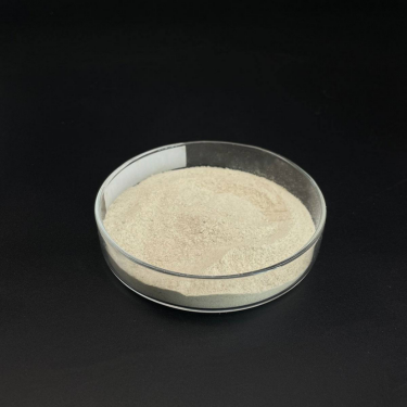
(Nano-Silicon Powder)
Nano-silicon powder, made up of silicon bits with particular measurements listed below 100 nanometers, represents a paradigm shift from bulk silicon in both physical actions and practical energy.
While bulk silicon is an indirect bandgap semiconductor with a bandgap of approximately 1.12 eV, nano-sizing generates quantum arrest results that fundamentally change its digital and optical residential or commercial properties.
When the bit size approaches or drops below the exciton Bohr span of silicon (~ 5 nm), charge carriers end up being spatially restricted, resulting in a widening of the bandgap and the introduction of noticeable photoluminescence– a phenomenon absent in macroscopic silicon.
This size-dependent tunability makes it possible for nano-silicon to produce light throughout the noticeable spectrum, making it an appealing prospect for silicon-based optoelectronics, where standard silicon falls short because of its poor radiative recombination performance.
Additionally, the raised surface-to-volume proportion at the nanoscale enhances surface-related sensations, including chemical reactivity, catalytic task, and communication with magnetic fields.
These quantum effects are not merely scholastic interests yet form the foundation for next-generation applications in power, noticing, and biomedicine.
1.2 Morphological Diversity and Surface Chemistry
Nano-silicon powder can be manufactured in numerous morphologies, including spherical nanoparticles, nanowires, permeable nanostructures, and crystalline quantum dots, each offering unique benefits relying on the target application.
Crystalline nano-silicon usually preserves the diamond cubic structure of bulk silicon but displays a greater density of surface problems and dangling bonds, which must be passivated to maintain the material.
Surface area functionalization– usually accomplished with oxidation, hydrosilylation, or ligand accessory– plays an essential duty in identifying colloidal security, dispersibility, and compatibility with matrices in composites or biological atmospheres.
For example, hydrogen-terminated nano-silicon reveals high sensitivity and is susceptible to oxidation in air, whereas alkyl- or polyethylene glycol (PEG)-layered particles display improved security and biocompatibility for biomedical usage.
( Nano-Silicon Powder)
The visibility of a native oxide layer (SiOₓ) on the particle surface area, even in very little amounts, significantly influences electric conductivity, lithium-ion diffusion kinetics, and interfacial responses, especially in battery applications.
Understanding and controlling surface area chemistry is consequently vital for utilizing the complete capacity of nano-silicon in sensible systems.
2. Synthesis Approaches and Scalable Construction Techniques
2.1 Top-Down Techniques: Milling, Etching, and Laser Ablation
The production of nano-silicon powder can be broadly classified right into top-down and bottom-up methods, each with distinctive scalability, pureness, and morphological control characteristics.
Top-down strategies entail the physical or chemical decrease of mass silicon right into nanoscale pieces.
High-energy round milling is a commonly made use of commercial approach, where silicon portions undergo extreme mechanical grinding in inert environments, resulting in micron- to nano-sized powders.
While cost-efficient and scalable, this method usually introduces crystal flaws, contamination from milling media, and wide bit size distributions, calling for post-processing filtration.
Magnesiothermic reduction of silica (SiO ₂) followed by acid leaching is an additional scalable path, particularly when making use of natural or waste-derived silica sources such as rice husks or diatoms, using a sustainable pathway to nano-silicon.
Laser ablation and responsive plasma etching are a lot more specific top-down methods, efficient in generating high-purity nano-silicon with regulated crystallinity, however at greater cost and reduced throughput.
2.2 Bottom-Up Techniques: Gas-Phase and Solution-Phase Development
Bottom-up synthesis permits higher control over fragment dimension, shape, and crystallinity by building nanostructures atom by atom.
Chemical vapor deposition (CVD) and plasma-enhanced CVD (PECVD) allow the growth of nano-silicon from gaseous forerunners such as silane (SiH FOUR) or disilane (Si two H SIX), with specifications like temperature, stress, and gas circulation dictating nucleation and development kinetics.
These methods are particularly efficient for producing silicon nanocrystals embedded in dielectric matrices for optoelectronic tools.
Solution-phase synthesis, consisting of colloidal paths utilizing organosilicon compounds, enables the production of monodisperse silicon quantum dots with tunable emission wavelengths.
Thermal disintegration of silane in high-boiling solvents or supercritical fluid synthesis also produces top quality nano-silicon with narrow size distributions, ideal for biomedical labeling and imaging.
While bottom-up approaches usually generate premium material high quality, they face obstacles in massive production and cost-efficiency, requiring continuous research into hybrid and continuous-flow procedures.
3. Power Applications: Changing Lithium-Ion and Beyond-Lithium Batteries
3.1 Function in High-Capacity Anodes for Lithium-Ion Batteries
Among one of the most transformative applications of nano-silicon powder hinges on energy storage space, particularly as an anode product in lithium-ion batteries (LIBs).
Silicon offers an academic specific capability of ~ 3579 mAh/g based on the formation of Li ₁₅ Si ₄, which is virtually ten times greater than that of traditional graphite (372 mAh/g).
Nevertheless, the big quantity growth (~ 300%) during lithiation creates particle pulverization, loss of electrical contact, and continual solid electrolyte interphase (SEI) development, causing rapid ability discolor.
Nanostructuring mitigates these concerns by reducing lithium diffusion courses, accommodating pressure better, and decreasing crack chance.
Nano-silicon in the form of nanoparticles, porous structures, or yolk-shell frameworks makes it possible for reversible biking with boosted Coulombic effectiveness and cycle life.
Commercial battery technologies now incorporate nano-silicon blends (e.g., silicon-carbon composites) in anodes to improve energy density in consumer electronics, electrical vehicles, and grid storage systems.
3.2 Potential in Sodium-Ion, Potassium-Ion, and Solid-State Batteries
Beyond lithium-ion systems, nano-silicon is being checked out in arising battery chemistries.
While silicon is less responsive with sodium than lithium, nano-sizing boosts kinetics and makes it possible for minimal Na ⁺ insertion, making it a candidate for sodium-ion battery anodes, particularly when alloyed or composited with tin or antimony.
In solid-state batteries, where mechanical stability at electrode-electrolyte user interfaces is vital, nano-silicon’s ability to go through plastic deformation at small scales decreases interfacial tension and boosts call maintenance.
Additionally, its compatibility with sulfide- and oxide-based strong electrolytes opens up avenues for much safer, higher-energy-density storage remedies.
Research continues to optimize user interface design and prelithiation techniques to take full advantage of the longevity and performance of nano-silicon-based electrodes.
4. Emerging Frontiers in Photonics, Biomedicine, and Composite Materials
4.1 Applications in Optoelectronics and Quantum Light Sources
The photoluminescent homes of nano-silicon have rejuvenated efforts to establish silicon-based light-emitting gadgets, an enduring challenge in integrated photonics.
Unlike bulk silicon, nano-silicon quantum dots can exhibit effective, tunable photoluminescence in the visible to near-infrared range, allowing on-chip light sources compatible with corresponding metal-oxide-semiconductor (CMOS) technology.
These nanomaterials are being integrated right into light-emitting diodes (LEDs), photodetectors, and waveguide-coupled emitters for optical interconnects and picking up applications.
Additionally, surface-engineered nano-silicon shows single-photon exhaust under specific defect arrangements, positioning it as a potential system for quantum information processing and safe interaction.
4.2 Biomedical and Ecological Applications
In biomedicine, nano-silicon powder is gaining attention as a biocompatible, biodegradable, and non-toxic option to heavy-metal-based quantum dots for bioimaging and drug shipment.
Surface-functionalized nano-silicon particles can be designed to target details cells, release restorative agents in feedback to pH or enzymes, and offer real-time fluorescence tracking.
Their degradation right into silicic acid (Si(OH)FOUR), a normally taking place and excretable compound, decreases lasting poisoning problems.
Furthermore, nano-silicon is being examined for environmental removal, such as photocatalytic destruction of pollutants under noticeable light or as a minimizing representative in water treatment processes.
In composite materials, nano-silicon boosts mechanical toughness, thermal stability, and use resistance when integrated right into metals, porcelains, or polymers, especially in aerospace and auto components.
To conclude, nano-silicon powder stands at the intersection of fundamental nanoscience and industrial innovation.
Its distinct combination of quantum effects, high reactivity, and versatility across energy, electronics, and life sciences underscores its function as a crucial enabler of next-generation innovations.
As synthesis methods advance and combination difficulties are overcome, nano-silicon will certainly remain to drive progression towards higher-performance, sustainable, and multifunctional product systems.
5. Supplier
TRUNNANO is a supplier of Spherical Tungsten Powder with over 12 years of experience in nano-building energy conservation and nanotechnology development. It accepts payment via Credit Card, T/T, West Union and Paypal. Trunnano will ship the goods to customers overseas through FedEx, DHL, by air, or by sea. If you want to know more about Spherical Tungsten Powder, please feel free to contact us and send an inquiry(sales5@nanotrun.com).
Tags: Nano-Silicon Powder, Silicon Powder, Silicon
All articles and pictures are from the Internet. If there are any copyright issues, please contact us in time to delete.
Inquiry us