1. Material Fundamentals and Architectural Attributes of Alumina Ceramics
1.1 Crystallographic and Compositional Basis of α-Alumina
(Alumina Ceramic Substrates)
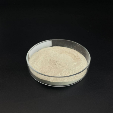
Alumina ceramic substratums, mostly composed of aluminum oxide (Al two O FIVE), serve as the foundation of modern-day digital packaging because of their phenomenal equilibrium of electrical insulation, thermal security, mechanical stamina, and manufacturability.
The most thermodynamically steady stage of alumina at high temperatures is corundum, or α-Al ₂ O ₃, which takes shape in a hexagonal close-packed oxygen lattice with light weight aluminum ions occupying two-thirds of the octahedral interstitial sites.
This thick atomic arrangement imparts high solidity (Mohs 9), exceptional wear resistance, and solid chemical inertness, making α-alumina appropriate for extreme operating settings.
Industrial substratums typically have 90– 99.8% Al Two O ₃, with minor additions of silica (SiO ₂), magnesia (MgO), or unusual earth oxides used as sintering help to advertise densification and control grain development throughout high-temperature handling.
Greater pureness grades (e.g., 99.5% and over) exhibit superior electric resistivity and thermal conductivity, while reduced pureness variations (90– 96%) use cost-efficient remedies for less requiring applications.
1.2 Microstructure and Problem Design for Electronic Reliability
The efficiency of alumina substratums in electronic systems is critically depending on microstructural harmony and flaw minimization.
A fine, equiaxed grain structure– normally varying from 1 to 10 micrometers– ensures mechanical honesty and reduces the possibility of crack proliferation under thermal or mechanical anxiety.
Porosity, especially interconnected or surface-connected pores, must be minimized as it degrades both mechanical toughness and dielectric efficiency.
Advanced processing methods such as tape casting, isostatic pushing, and controlled sintering in air or managed atmospheres allow the manufacturing of substratums with near-theoretical thickness (> 99.5%) and surface area roughness listed below 0.5 µm, essential for thin-film metallization and wire bonding.
Additionally, impurity partition at grain boundaries can result in leakage currents or electrochemical movement under predisposition, necessitating strict control over resources purity and sintering conditions to make sure long-lasting integrity in moist or high-voltage environments.
2. Manufacturing Processes and Substratum Manufacture Technologies
( Alumina Ceramic Substrates)
2.1 Tape Casting and Environment-friendly Body Handling
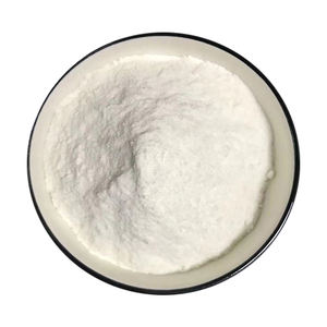
The production of alumina ceramic substratums begins with the preparation of a highly dispersed slurry including submicron Al two O two powder, natural binders, plasticizers, dispersants, and solvents.
This slurry is refined using tape casting– a continuous approach where the suspension is spread over a relocating service provider film making use of a precision doctor blade to accomplish consistent density, commonly in between 0.1 mm and 1.0 mm.
After solvent evaporation, the resulting “eco-friendly tape” is versatile and can be punched, drilled, or laser-cut to form via holes for vertical interconnections.
Multiple layers might be laminated flooring to develop multilayer substratums for complicated circuit combination, although the majority of commercial applications utilize single-layer arrangements because of set you back and thermal development considerations.
The green tapes are then meticulously debound to get rid of natural ingredients through managed thermal disintegration prior to final sintering.
2.2 Sintering and Metallization for Circuit Assimilation
Sintering is conducted in air at temperatures in between 1550 ° C and 1650 ° C, where solid-state diffusion drives pore elimination and grain coarsening to accomplish complete densification.
The direct contraction during sintering– normally 15– 20%– have to be specifically anticipated and made up for in the style of eco-friendly tapes to make certain dimensional precision of the final substratum.
Adhering to sintering, metallization is put on develop conductive traces, pads, and vias.
Two main methods control: thick-film printing and thin-film deposition.
In thick-film modern technology, pastes containing metal powders (e.g., tungsten, molybdenum, or silver-palladium alloys) are screen-printed onto the substratum and co-fired in a lowering environment to form robust, high-adhesion conductors.
For high-density or high-frequency applications, thin-film procedures such as sputtering or evaporation are used to down payment attachment layers (e.g., titanium or chromium) adhered to by copper or gold, allowing sub-micron patterning via photolithography.
Vias are full of conductive pastes and terminated to develop electrical affiliations between layers in multilayer designs.
3. Useful Features and Efficiency Metrics in Electronic Solution
3.1 Thermal and Electric Behavior Under Operational Anxiety
Alumina substratums are prized for their desirable mix of modest thermal conductivity (20– 35 W/m · K for 96– 99.8% Al ₂ O SIX), which enables reliable heat dissipation from power tools, and high volume resistivity (> 10 ¹⁴ Ω · centimeters), making certain marginal leak current.
Their dielectric continuous (εᵣ ≈ 9– 10 at 1 MHz) is steady over a wide temperature and frequency range, making them ideal for high-frequency circuits as much as numerous ghzs, although lower-κ materials like aluminum nitride are liked for mm-wave applications.
The coefficient of thermal growth (CTE) of alumina (~ 6.8– 7.2 ppm/K) is reasonably well-matched to that of silicon (~ 3 ppm/K) and specific product packaging alloys, lowering thermo-mechanical stress and anxiety during tool procedure and thermal cycling.
However, the CTE mismatch with silicon continues to be an issue in flip-chip and direct die-attach configurations, often needing certified interposers or underfill products to minimize tiredness failure.
3.2 Mechanical Toughness and Ecological Sturdiness
Mechanically, alumina substrates display high flexural toughness (300– 400 MPa) and exceptional dimensional security under tons, allowing their use in ruggedized electronic devices for aerospace, automotive, and commercial control systems.
They are resistant to vibration, shock, and creep at elevated temperatures, maintaining structural stability up to 1500 ° C in inert ambiences.
In moist atmospheres, high-purity alumina shows minimal moisture absorption and superb resistance to ion movement, making sure lasting integrity in outside and high-humidity applications.
Surface area hardness additionally protects versus mechanical damages throughout handling and assembly, although treatment must be required to avoid edge damaging due to integral brittleness.
4. Industrial Applications and Technical Effect Throughout Sectors
4.1 Power Electronics, RF Modules, and Automotive Solutions
Alumina ceramic substrates are ubiquitous in power digital modules, consisting of insulated gate bipolar transistors (IGBTs), MOSFETs, and rectifiers, where they offer electric seclusion while helping with warm transfer to warmth sinks.
In radio frequency (RF) and microwave circuits, they work as service provider systems for hybrid integrated circuits (HICs), surface area acoustic wave (SAW) filters, and antenna feed networks as a result of their secure dielectric residential or commercial properties and reduced loss tangent.
In the automotive industry, alumina substratums are used in engine control units (ECUs), sensor plans, and electrical car (EV) power converters, where they sustain high temperatures, thermal biking, and exposure to destructive liquids.
Their dependability under severe problems makes them crucial for safety-critical systems such as anti-lock stopping (ABDOMINAL) and progressed driver assistance systems (ADAS).
4.2 Clinical Devices, Aerospace, and Emerging Micro-Electro-Mechanical Equipments
Beyond customer and commercial electronics, alumina substratums are used in implantable medical gadgets such as pacemakers and neurostimulators, where hermetic sealing and biocompatibility are vital.
In aerospace and defense, they are made use of in avionics, radar systems, and satellite interaction components due to their radiation resistance and security in vacuum cleaner atmospheres.
Furthermore, alumina is significantly utilized as a structural and insulating platform in micro-electro-mechanical systems (MEMS), consisting of pressure sensors, accelerometers, and microfluidic devices, where its chemical inertness and compatibility with thin-film processing are helpful.
As electronic systems remain to require higher power densities, miniaturization, and integrity under severe problems, alumina ceramic substrates remain a cornerstone material, connecting the gap in between performance, cost, and manufacturability in advanced digital packaging.
5. Supplier
Alumina Technology Co., Ltd focus on the research and development, production and sales of aluminum oxide powder, aluminum oxide products, aluminum oxide crucible, etc., serving the electronics, ceramics, chemical and other industries. Since its establishment in 2005, the company has been committed to providing customers with the best products and services. If you are looking for high quality alumina casting, please feel free to contact us. (nanotrun@yahoo.com)
Tags: Alumina Ceramic Substrates, Alumina Ceramics, alumina
All articles and pictures are from the Internet. If there are any copyright issues, please contact us in time to delete.
Inquiry us