1. Crystal Framework and Polytypism of Silicon Carbide
1.1 Cubic and Hexagonal Polytypes: From 3C to 6H and Past
(Silicon Carbide Ceramics)
Silicon carbide (SiC) is a covalently adhered ceramic composed of silicon and carbon atoms organized in a tetrahedral coordination, developing among one of the most complicated systems of polytypism in materials scientific research.
Unlike most porcelains with a solitary stable crystal framework, SiC exists in over 250 recognized polytypes– distinct stacking sequences of close-packed Si-C bilayers along the c-axis– ranging from cubic 3C-SiC (also known as β-SiC) to hexagonal 6H-SiC and rhombohedral 15R-SiC.
One of the most typical polytypes utilized in design applications are 3C (cubic), 4H, and 6H (both hexagonal), each displaying a little different electronic band structures and thermal conductivities.
3C-SiC, with its zinc blende structure, has the narrowest bandgap (~ 2.3 eV) and is generally grown on silicon substratums for semiconductor devices, while 4H-SiC supplies remarkable electron movement and is liked for high-power electronics.
The solid covalent bonding and directional nature of the Si– C bond give outstanding firmness, thermal stability, and resistance to sneak and chemical assault, making SiC perfect for extreme setting applications.
1.2 Flaws, Doping, and Electronic Quality
In spite of its architectural complexity, SiC can be doped to attain both n-type and p-type conductivity, enabling its use in semiconductor gadgets.
Nitrogen and phosphorus function as contributor impurities, introducing electrons into the conduction band, while aluminum and boron serve as acceptors, producing holes in the valence band.
Nonetheless, p-type doping efficiency is restricted by high activation powers, particularly in 4H-SiC, which postures obstacles for bipolar tool layout.
Native problems such as screw dislocations, micropipes, and piling faults can break down device efficiency by acting as recombination facilities or leak paths, necessitating high-grade single-crystal growth for digital applications.
The broad bandgap (2.3– 3.3 eV relying on polytype), high failure electrical area (~ 3 MV/cm), and exceptional thermal conductivity (~ 3– 4 W/m · K for 4H-SiC) make SiC much above silicon in high-temperature, high-voltage, and high-frequency power electronics.
2. Processing and Microstructural Engineering
( Silicon Carbide Ceramics)
2.1 Sintering and Densification Techniques
Silicon carbide is naturally challenging to compress because of its solid covalent bonding and reduced self-diffusion coefficients, calling for innovative handling approaches to accomplish complete density without additives or with minimal sintering help.
Pressureless sintering of submicron SiC powders is feasible with the addition of boron and carbon, which advertise densification by removing oxide layers and improving solid-state diffusion.
Hot pushing applies uniaxial pressure during home heating, allowing complete densification at lower temperature levels (~ 1800– 2000 ° C )and producing fine-grained, high-strength parts ideal for cutting tools and put on parts.
For big or intricate shapes, reaction bonding is employed, where porous carbon preforms are infiltrated with liquified silicon at ~ 1600 ° C, developing β-SiC in situ with very little shrinking.
However, recurring totally free silicon (~ 5– 10%) remains in the microstructure, restricting high-temperature efficiency and oxidation resistance above 1300 ° C.
2.2 Additive Production and Near-Net-Shape Construction
Recent advancements in additive manufacturing (AM), specifically binder jetting and stereolithography utilizing SiC powders or preceramic polymers, allow the construction of complicated geometries previously unattainable with standard methods.
In polymer-derived ceramic (PDC) paths, fluid SiC precursors are shaped by means of 3D printing and then pyrolyzed at high temperatures to produce amorphous or nanocrystalline SiC, often calling for more densification.
These techniques reduce machining costs and product waste, making SiC much more easily accessible for aerospace, nuclear, and warm exchanger applications where complex layouts enhance performance.
Post-processing steps such as chemical vapor infiltration (CVI) or liquid silicon infiltration (LSI) are in some cases made use of to improve thickness and mechanical integrity.
3. Mechanical, Thermal, and Environmental Performance
3.1 Toughness, Solidity, and Use Resistance
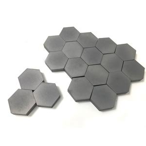
Silicon carbide ranks among the hardest known materials, with a Mohs hardness of ~ 9.5 and Vickers firmness exceeding 25 GPa, making it very resistant to abrasion, disintegration, and scratching.
Its flexural stamina normally ranges from 300 to 600 MPa, relying on processing method and grain size, and it keeps strength at temperature levels up to 1400 ° C in inert environments.
Fracture strength, while moderate (~ 3– 4 MPa · m ¹/ ²), is sufficient for many architectural applications, especially when integrated with fiber reinforcement in ceramic matrix compounds (CMCs).
SiC-based CMCs are used in generator blades, combustor liners, and brake systems, where they provide weight cost savings, gas performance, and extended life span over metallic equivalents.
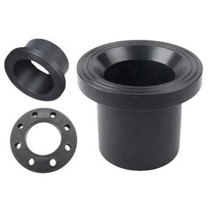
Its outstanding wear resistance makes SiC perfect for seals, bearings, pump components, and ballistic armor, where longevity under severe mechanical loading is important.
3.2 Thermal Conductivity and Oxidation Security
Among SiC’s most important homes is its high thermal conductivity– approximately 490 W/m · K for single-crystal 4H-SiC and ~ 30– 120 W/m · K for polycrystalline forms– going beyond that of several steels and allowing efficient heat dissipation.
This building is critical in power electronic devices, where SiC devices produce much less waste heat and can operate at higher power densities than silicon-based gadgets.
At raised temperatures in oxidizing atmospheres, SiC develops a safety silica (SiO ₂) layer that reduces further oxidation, giving excellent environmental resilience up to ~ 1600 ° C.
Nonetheless, in water vapor-rich atmospheres, this layer can volatilize as Si(OH)FOUR, leading to accelerated degradation– an essential challenge in gas generator applications.
4. Advanced Applications in Power, Electronics, and Aerospace
4.1 Power Electronics and Semiconductor Instruments
Silicon carbide has actually revolutionized power electronic devices by making it possible for tools such as Schottky diodes, MOSFETs, and JFETs that operate at greater voltages, regularities, and temperatures than silicon equivalents.
These tools lower energy losses in electric cars, renewable resource inverters, and commercial electric motor drives, contributing to worldwide power performance renovations.
The ability to operate at joint temperatures above 200 ° C permits simplified air conditioning systems and boosted system dependability.
In addition, SiC wafers are made use of as substratums for gallium nitride (GaN) epitaxy in high-electron-mobility transistors (HEMTs), incorporating the advantages of both wide-bandgap semiconductors.
4.2 Nuclear, Aerospace, and Optical Equipments
In nuclear reactors, SiC is a crucial part of accident-tolerant fuel cladding, where its reduced neutron absorption cross-section, radiation resistance, and high-temperature stamina enhance safety and efficiency.
In aerospace, SiC fiber-reinforced composites are utilized in jet engines and hypersonic vehicles for their lightweight and thermal stability.
Additionally, ultra-smooth SiC mirrors are utilized precede telescopes as a result of their high stiffness-to-density ratio, thermal stability, and polishability to sub-nanometer roughness.
In summary, silicon carbide ceramics stand for a cornerstone of modern advanced materials, integrating remarkable mechanical, thermal, and electronic buildings.
With accurate control of polytype, microstructure, and handling, SiC continues to allow technological developments in power, transportation, and extreme atmosphere engineering.
5. Supplier
TRUNNANO is a supplier of Spherical Tungsten Powder with over 12 years of experience in nano-building energy conservation and nanotechnology development. It accepts payment via Credit Card, T/T, West Union and Paypal. Trunnano will ship the goods to customers overseas through FedEx, DHL, by air, or by sea. If you want to know more about Spherical Tungsten Powder, please feel free to contact us and send an inquiry(sales5@nanotrun.com).
Tags: silicon carbide ceramic,silicon carbide ceramic products, industry ceramic
All articles and pictures are from the Internet. If there are any copyright issues, please contact us in time to delete.
Inquiry us